Difference between revisions of "Modify the Linksys hardware"
| Line 109: | Line 109: | ||
[[Image:Completed transceiver.jpg|thumb|400px|left|Complete transceiver board with all components in place.]] | [[Image:Completed transceiver.jpg|thumb|400px|left|Complete transceiver board with all components in place.]] | ||
| − | The next step is to | + | The next step is to build the transceiver circuit, which converts the 3.3 volt serial signals from the router to conventional RS-232 serial voltages. The circuit includes only a handful of components, so it can be assembled using a small square of "perf board", or a variety of other inexpensive circuit prototyping techniques. We use a custom-made printed circuit board to simplify assembly, as shown here. (Link to page with PCB specs, and directions.) Again, you'll need your '''soldering iron''' to secure the different pieces in the transceiver board. |
| − | |||
| − | |||
| − | |||
| − | |||
| + | Using the diagram on the left, solder the '''shrouded double header''', the '''socket''', and the '''capacitors''' into the board in the appropriate places. '''NOTE:''' the positions of the components on the physical board are not represented in the diagram, but the silkscreen on the board indicates placement and orientation. '''FURTHER NOTE:''' each component has a proper polarity or pin marking -- direction matters! | ||
| + | The pictures to the right show the transceiver board in various stages of completion. The top one shows the blank board on which the other components will be added. The bottom one shows the '''shrouded double header''', the '''socket''', and the '''capacitors''' soldered in place. It also shows the actual ADM202 chip inserted into the socket. The next step is to get six wires from a chopped up piece of the ribbon cable (or any six spare wires) and solder them into place in the six holes (two sets of three) at the bottom of the transceiver board. The resulting completed transceiver board should look something like the picture below the diagram. | ||
<h3 style="clear:both;"> Task Four: Attach Tranceiver Board to the Router</h3> | <h3 style="clear:both;"> Task Four: Attach Tranceiver Board to the Router</h3> | ||
Revision as of 15:19, 26 June 2008
Summary
This will walk through adding hardware to a Linksys WRT54GL wireless router that will take advantage of existing connections on the PCB for two UART connections, which will be exposed as DB9 serial port connectors mounted to the faceplate of the router. These connections can be used to communicate with the serial console for XINU and also to interact with the Common Firmware Environment's command line interface. Gaining direct access to CFE is a key step towards being able to run XINU on the router.
Before Starting
Parts List
| Quantity | Part Name | Details | Part / Model Number | Price |
|---|---|---|---|---|
| 1 | LinkSys WRT54GL Router | 802.11b/g wireless broadband router | Linksys WRT54GL | ~$65.00 |
| 1 | Ribbon cable | 28 AWG, 10 conductor, 25' | Jameco 643508CM | $4.99 |
| 2 | IDC socket connector | 0.1”, 10 conductor | Jameco 32491CM | $0.25 |
| 2 | IDC shrouded double header | 0.1”, 10 conductor | Jameco 67811CM | $0.33 |
| 1 | ADM202 Transceiver Chip | ????????????? | ????????????? | $?.?? |
| 2 | Capacitor 220 nF | ????????????? | ????????????? | $?.?? |
| 3 | Capacitor 100 nF | ????????????? | ????????????? | $?.?? |
| 1 | Transceiver Board | ????????????? | ????????????? | $?.?? |
| 1 | DB9 Female | 22AWG,SOLDER CUP | Jameco 15771CM | $0.59 |
| 1 | DB9 Male | 22AWG,SOLDER CUP | Jameco 15747CM | $0.59 |
(We provide this parts list as a data point; we offer no guarantees about current prices, and it is not our intent to endorse any particular vendor.)
Tools List
- Soldering Iron
- Dremel tool (for cutting holes in plastic case)
- Continuity Tester (Multimeter, or some other way of checking for proper connections)
Steps to Modify the Hardware
Task One: Open the Router
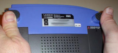
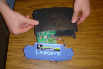
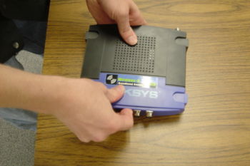
There are no screws or tools needed to open the router, just pop open the front with your thumbs as shown in the picture. Some nice illustrated opening instructions can be found for a more detailed explanation of this step
DO NOTE: This is where the warranty on the router is voided!
Task Two: Attach the Serial Header
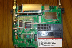
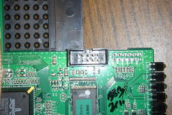
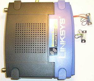
Once the PCB has been removed from the case, locate the serial header holes provided by LinkSys. This would be a grid of 10 holes (5x2) located on the bottom-right corner of the board when the antennae stubs are on top (see the top-down photo for clarification). These ten holes hold all of the input and output for the two serial interfaces--UART0, and UART1--on the device.
Now, we could just solder wires right onto these holes, but a by placing a nice 10-pin header on the board we can easily attach and detach a 10 connection cable. Here you will use your soldering iron to solder the IDC shrouded double header onto the board.
Task Three: Create the ADM202 Transceiver Circuit Board
The next step is to build the transceiver circuit, which converts the 3.3 volt serial signals from the router to conventional RS-232 serial voltages. The circuit includes only a handful of components, so it can be assembled using a small square of "perf board", or a variety of other inexpensive circuit prototyping techniques. We use a custom-made printed circuit board to simplify assembly, as shown here. (Link to page with PCB specs, and directions.) Again, you'll need your soldering iron to secure the different pieces in the transceiver board.
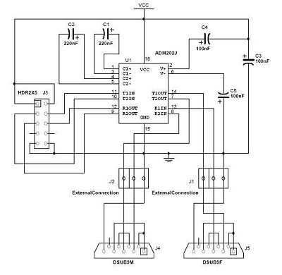
Using the diagram on the left, solder the shrouded double header, the socket, and the capacitors into the board in the appropriate places. NOTE: the positions of the components on the physical board are not represented in the diagram, but the silkscreen on the board indicates placement and orientation. FURTHER NOTE: each component has a proper polarity or pin marking -- direction matters!
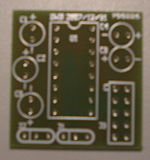
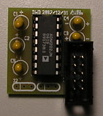
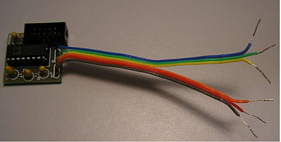
The pictures to the right show the transceiver board in various stages of completion. The top one shows the blank board on which the other components will be added. The bottom one shows the shrouded double header, the socket, and the capacitors soldered in place. It also shows the actual ADM202 chip inserted into the socket. The next step is to get six wires from a chopped up piece of the ribbon cable (or any six spare wires) and solder them into place in the six holes (two sets of three) at the bottom of the transceiver board. The resulting completed transceiver board should look something like the picture below the diagram.
Task Four: Attach Tranceiver Board to the Router
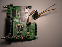
First take a piece of ribbon cable and attach each end to one of your IDC socket connectors. Then attach one connector to the header we soldered into the router's board and the other connector to the header we soldered into the transceiver board. The result should look something like the picture to the left.
Task Five: Attach Transceiver Board to DB9 Serial Ports
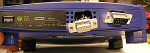
Before soldering the wires from the transceiver board to the serial ports, it is a good idea to drill two holes in the front of the router's casing to use for the serial ports. The three pictures to the right show how to take off the front sticker and what the case should look like after you've drilled two holes in the front for the serial ports. It is also a good idea to cut the sticker and place the left part back on to cover up the remaining holes in the casing.
Next, feed the six wires coming from the transceiver board through the two holes you just drilled. Make sure that the three wires soldered into the holes marked J1 on the transceiver board go through the hole on the left of the front of the router and the three wires soldered into the holes marked J2 on the transceiver board go through the hole on the right of the front of the router.
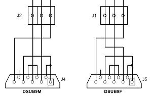
Following the diagram to the left, solder some spare wires or chopped pieces of ribbon cable into the two DB9 serial ports. Notice that solder cups 1, 4, and 6 are connected to each other and solder cups 7 and 8 are connected to each other on both the DB9 Female and DB9 Male serial ports. Then, again following the diagram, solder in the wires coming from J1 into the appropriate solder cups of the DB9 Female and the wires coming from J2 into the appropriate solder cups of the DB9 Male.
Notice that in the case of the DB9 Female the T1OUT pin of the ADM202 transceiver chip needs to be connected to solder cup 2, the R1IN pin of the ADM202 transceiver chip needs to be connected to solder cup 3, and the ground needs to be connected to solder cup 5.
Also, notice that in the case of the DB9 Male the R2IN pin of the ADM202 transceiver chip needs to be connected to solder cup 2, the T2OUT pin of the ADM202 transceiver chip needs to be connected to solder cup 3, and the ground needs to be connected to solder cup 5.
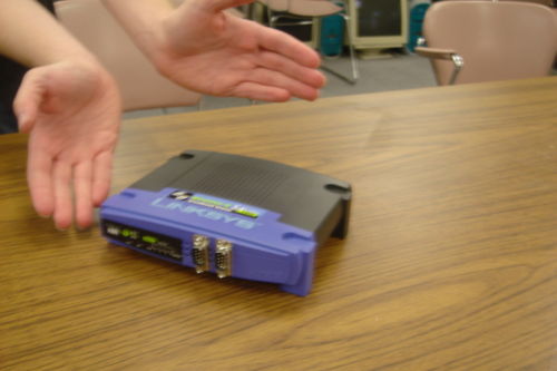
Feeding the wires through the holes and connecting the serial ports in this way ensures that the router's primary serial device will be connected to the DB9 Female serial port and will be located on the left side while the router's secondary serial device will be connected to the DB9 Male serial port and will be located on the right side of the front of the router.
After all the soldering is done it is a good idea to use a continuity tester to make sure that all the connections are good and no wires or solder cups may be accidentally touching. Your final result should look something like the pictures below.
Task Six: Close the Router
This final task is best described in photos:
Task Seven: Rejoice
What to do next?
Connect UART0 (the DB9 Female serial port) to a computer and follow the next HOWTO on using a PC to connect to a modified router.
This work is supported in part by NSF grant DUE-CCLI-0737476.
